75-學術專欄:陳福榮老師專文
學術專欄:奈米晶體原子分辨率的三維全息術實現了費曼的夢想---嶄新三維原子分辨率的電子顯微學
◎文/清華工科系 陳福榮教授
在1950年奈米科技之父費曼大師在他很有名的演講<there is a plenty of room at the bottom>中提出了他的夢想:「若是我們能夠觀察到原子在三維空間上的位置,那麼再複雜的化學物質的分析將變得非常簡單」。而我們這一篇Nature Communications 文章中提出了一個嶄新的電子顯微學實驗及理論方法,實現了費曼的夢想。
我們這次很榮幸與美國勞倫茲國家實驗室電子顯微鏡中心Christian Kisielowski敎授及比利時安特衛普大學Dirk Van Dyck教授在共同發表的Nature Communications 文章中,合作利用低劑量的電子顯微術,在不破壞奈米材料的條件下,重構出奈米顆粒電子全息像。並且發展全新3D電子顯微理論,由電子全息像,以幾近0.1奈米的準確度萃取出奈米顆粒表面的原子分辨的形貌,及沿著電子束投影方向定量數原子,以單一原子準確度定量奈米顆粒的厚度。在文章中展示了奈米鍺晶,奈米金橋及奈米氧化鎂顆粒的原子分辨率的三維斷層結構。
在和美國勞倫茲國家實驗室電子顯微鏡中心Christian Kisielowski敎授及比利時安特衛普大學Dirk Van Dyck教授在共同發表的Nature Communications 文章中,提出了一個嶄新的電子顯微學實驗及理論方法,實現了費曼的夢想 :「若是我們能夠觀察到原子在三維空間上的位置,那麼再複雜的化學物質的分析將變得非常簡單」。
但是要達到費曼的夢想,基本上有兩個很重要的障礙。其一是現在最先進的電子顯微鏡分辨率足夠得到原子等級分辨率影像,但是只有二維投影結構,因為沿著電子束投影方向的原子的數目和結構全隱藏在投影的影像中,「就像拍照一樣,你只能看到有一排人,看不到他們之間前後距離有多遠。」。第二個障礙是電子輻射損傷會在影像拍攝過程中,改變奈米材料的結構,甚至產生破壞。
在這篇國際合作的文章中,無論在電子顯微鏡技術及理論都有創新的突破,在實驗方面,研究團隊發展利用低劑量的電子顯微術,在不破壞奈米材料的條件下,拍攝多張聚焦在不同焦平面的影像、以看出前後位置的原子結構;在理論上,由這一系列影像重構出髙訊號、低雜訊3D影像,再利用3D影像電子波的傳遞,量測奈米顆粒表面原子的位置。由此,可以決定原子分辨率的表面形貌,準確度高於0.1奈米。
我們研究從3D影像可以計數出投影方向的原子數目,奈米顆粒在電子束方向厚度的量測可以定量準確到一個原子。藉由表面形貌及準確計數原子個數,奈米顆粒的3D空間形狀就可以在原子分辨率的尺度下重建,完成費曼的夢想。
In the late 1950th Richard Feynman pointed out that, “It would be very easy to make an analysis of any complicated chemical substance; all one would have to do would be to look at it and see where the atoms are.” In principle, resolution and sensitivity of the latest generation aberration-corrected Transmission Electron Microscopes allow imaging the vast majority of single atoms from the Periodic Table of Elements with sub-Ångstrom resolution and determining their locations in an image plane with a precision that exceeds the 1.9 pm wavelength of 300 kV electrons. However, there are bottlenecks to achieve Feynman’s dream. A most noticeable bottleneck is the large accumulated electron dose required to produce tilt series of atomic resolution images because electron dose rates are commonly chosen large (104 - 105eÅ-2s-1) to achieve a needed resolution around one Ångstrom and single atom sensitivity. Any such single image can exhibit uncontrolled electron beam-induced surfaces alterations or even bulk modifications in particular if particles are small.
To address Feynman’s dream, an international research team, Professor Fu-Rong Chen (National Tsing-Hua University, Taiwan) , Professor Christian Kisielowski (National Centre for Electron Microscopy, Berkeley) and Professor Dirk Van Dyck (EMAT, University of Antwerp) has cooperated for many years to develop a general tomographic method to recover the 3D shape of a crystalline particle from high-resolution images of a single projection without need for sample rotation. The method is compatible with low dose rate electron microscopy, which improves on signal quality while minimizing electron beam-induced structure modifications even for small particles or surfaces. They apply it to Ge, Au and MgO particles and achieve a depth resolution of 1-2 Å, which is smaller than inter-atomic distances.
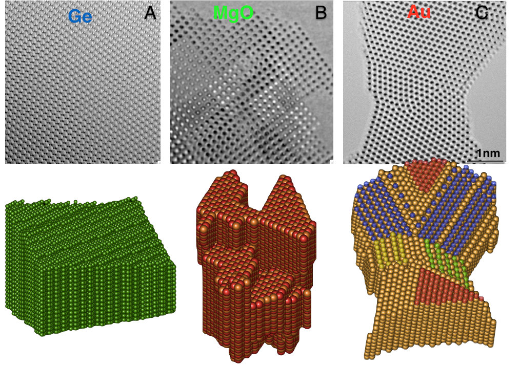
上排的圖(由左至右)是奈米鍺晶,氧化鎂奈米顆粒及金奈米橋的原子分辨率影像,下排的圖( 由左至右) 各為以上奈米顆粒重構的三維原子分辨率的斷層結構!